
The NFC Antenna Design Principle: From the size to match…
NFC (Near Field Communication) operate at a frequency of 13.56MHz and is widely used in access control,mobile payment, smart wearable, and electronic tags.
The NFC antenna design directly determines the read distance, stability,and reliability of the device.
This article will systematically review the NFC antenna design principle from three main dimensions: physical dimensions,electrical parameters,and environment adaptability.
I. The NFC physical dimensions and layout requirements
1.Area and shape
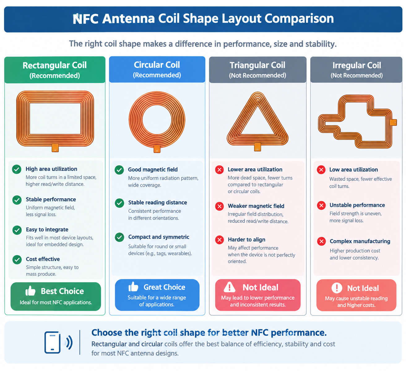
Area and Shape: When space permits, a larger antenna area results in greater magnetic flux and a longer communication distance. An effective area of around 1500 mm² is generally recommended.
Shape: Prioritize regular shapes such as squares or circles for uniform magnetic flux distribution; avoid irregular shapes such as L-shapes and U-shapes, as these can easily create reading dead zones.
Center Area: Keep the center of the coil as empty as possible, avoiding the placement of metal or magnetically conductive materials.
2.Line width and line spacing
Line width: Recommended range: 0.15mm ~ 1mm. Too narrow a trace width increases processing difficulty and DC resistance, while too wide a trace width affects the number of turns and inductance design.
Trace spacing (inter-turn gap): Recommended range: 0.15mm ~ 1mm. Too narrow a trace spacing increases parasitic coupling, while too wide a spacing wastes effective area. A comprehensive balance must be struck considering PCB/FPC processing precision.
3. Number of turns
The standard number of turns is 4-8 turns. More turns result in a larger inductance, but excessively large inductance can lead to an insufficient tuning capacitor (susceptible to parasitic parameters). A trade-off must be made between antenna area and inductance target.
4. Distance and Isolation (Focus on Metallic Environments):
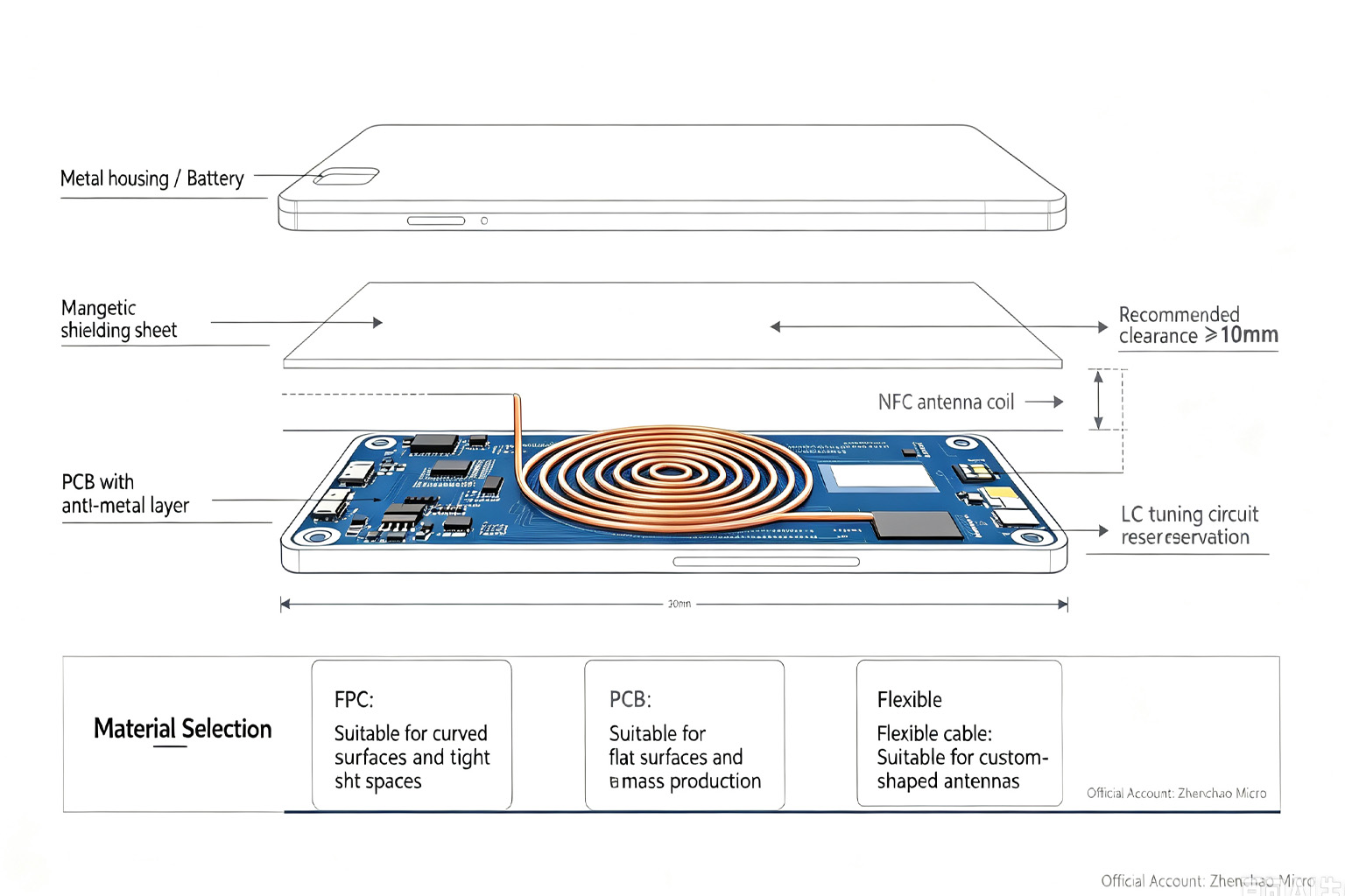
The antenna should be kept as far away as possible from metallic objects (such asbatteries, metal casings, and PCB ground planes). A distance of at least 10mm is recommended to avoid eddy currents in the metal, which can cause antenna, detuning, reduced inductance, and deteriorated Q-value.
II. The NFC Antenna Design Principle of the electrical parameter
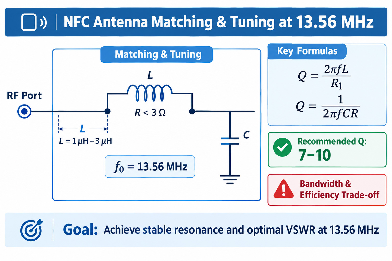
1. The target inductance (L) value is typically designed between 1μH and 3μH (optimal range is 1μH to 2μH) to achieve stable LC resonance at 13.56MHz through an external matching capacitor.
2.The recommended design range for the quality factor (Q value) is 7 to 10.
A high Q value results in narrower bandwidth, poor communication stability, and susceptibility to frequency drift.
A low Q value reduces energy transfer efficiency and shortens the reading distance. The Q value can be adjusted by connecting series/parallel resistors or by adjusting the coil structure.
3. The DC resistance (R) should be as low as possible, typically less than 3Ω, to reduce ohmic losses in the coil itself and improve transmission efficiency.
4. The resonant frequency must be precisely tuned to 13.56MHz (or 14.5~16MHz according to specific protocol requirements, such as 14.5~16MHz in card mode) through a matching capacitor to ensure optimal VSWR and maximum card reading distance at the target frequency.
III. Environmental and Process Requirements
1.Environmental Adaptation
When encountering the following situations, the following NFC antenna design principle can be referenced:
All-metal casing devices: Anti-metal design is essential (e.g., adding a ferrite isolation layer or adjusting the antenna position); otherwise, the antenna will hardly function properly.
Internal interference sources: Properly plan antenna wiring to avoid overlap or close parallel routing with internal high-frequency interference sources (such as clock circuits, RF power amplifiers, DC-DC converters).
Multiple antenna coexistence: If the device simultaneously has Bluetooth/WiFi/4G antennas, mutual interference needs to be assessed, and frequency division or spatial isolation design should be implemented if necessary.
2. Material selection:
Antenna materials should be flexibly chosen based on the equipment structure and assembly method.
FPC (Flexible Printed Circuit): Suitable for curved, irregularly shaped, or space-constrained equipment.
PCB (Rigid Printed Circuit): Suitable for planar structures and high-volume production equipment, offering good consistency. Enamelled wire wound coils: Suitable for customized, small-batch, or special-shaped coil designs, offering high flexibility.
A balance must be struck between processing accuracy, cost, and electrical performance.
3. Matching circuit reserved
The antenna port must have reserved layout space for the LC tuning circuit (usually a π-type or L-type structure). Debug pads (such as 0Ω resistors or test points) should also be reserved for later actual tuning using a Vector Network Analyzer (VNA) to compensate for frequency offset effects caused
by the device housing, parasitic capacitance, and layout deviations.